Non-invasive imaging of atomic arrangement at the sub-angstrom scale in 2-D hybrid perovskites
May 11, 2022 feature
by Thamarasee Jeewandara , Phys.org
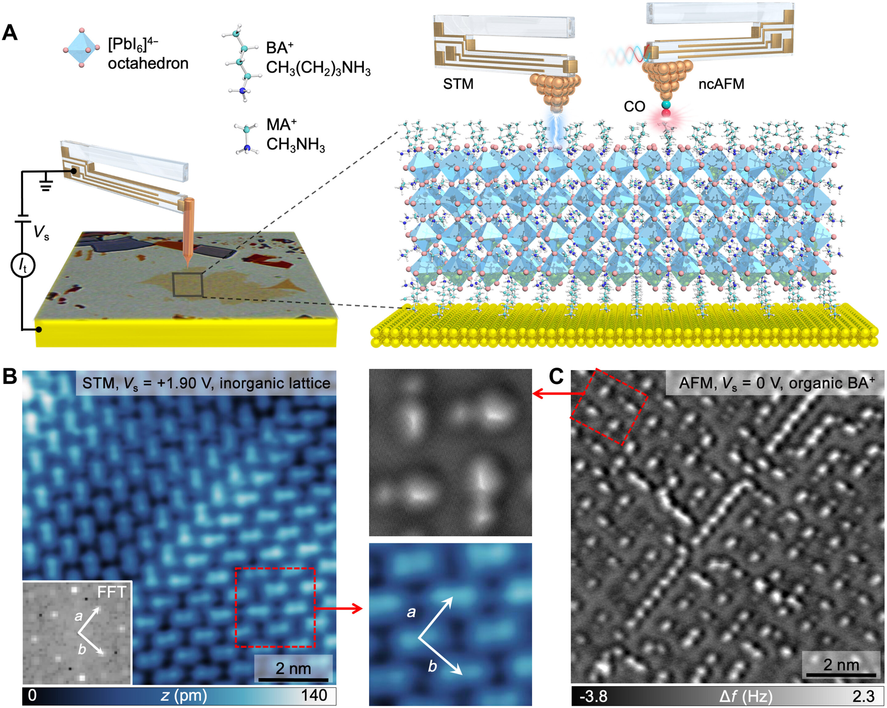
Materials scientists aim to identify the atomic arrangement of 2D Ruddlesden-Popper hybrid perovskites (RPP) using non-invasive imaging; however, the process is challenging due to the insulating nature and softness of the organic layers. In a new report now published in Science Advances, Mykola Telychko, Shayan Edaltmanesh, and Kai Leng, and a team of scientists in physics, chemistry, and materials at the National University of Singapore, and Palacky University Czech Republic, demonstrated sub-angstrom resolution imaging of soft organic layers and inorganic frameworks in a two-dimensional lead-halide perovskite crystal. The team accomplished this using scanning tunneling microscopy and noncontact atomic force microscopy supported with theoretical simulations. The scanning tunneling microscopy results unveiled the atomic reconstruction of the inorganic lead-halide lattice and composition of the crystal, while atomic force microscopy provided undisputed visualization of the materials surface and bonding interactions with the inorganic lattice. The joint method allowed the scientists to obtain atomic scale imaging and electrostatic potential of the material to reveal alternative quasi 1-D electron and hole channels at the neighboring twin boundaries.
The research team described two-dimensional hybrid perovskites as a remarkable platform for optoelectronic device applications. They credited the productivity of the platform to a close link between excitonic properties and quantum well structures of soft insulating organic layers sandwiched between conducting inorganic lead-halide frameworks. The presence of two-dimensionality led to the emergence of many quantum phenomena, while significantly enhancing photo and chemical stability and tunability of optoelectronic properties. Based on the unique dielectric and quantum effects, Telychko et al established the perovskites as a promising class of materials for next-generation optoelectronic applications. The team showed how the structural relaxation of inorganic lattices of 2D perovskites lead to the emergence of a variety of materials properties at the atomic scale in hybrid perovskites that had hitherto remained to be studied. To understand the influence of the lattice architecture on the inherent properties of interest, they used scanning tunneling microscopy and scanning transmission electron microscopy at first, but since some of these methods could cause structural damage via collisions of perovskites with the energetic beam. Telychko et al used recent advances in tuning fork (qPlus)-based non-contact atomic force microscopy (nCAFM) imaging with a carbon monoxide functionalized tip for atomically resolved studies. The methods provided an ideal tool for non-invasive sub-angstrom scale imaging of the perovskite crystals and their insulating organic layers.


/cdn.vox-cdn.com/uploads/chorus_asset/file/25417835/51684715392_2615642caa_o.jpg)


