Intel CPU with Optical Compute Interconnect Chiplet Demoed with 4Tbps of Bandwidth and 100m Reach
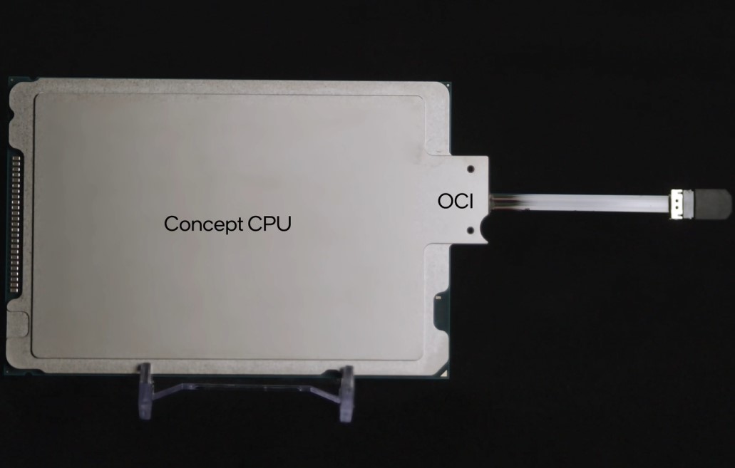
Intel showed off a pretty cool piece of technology integrating an optical I/O chiplet with a CPU. The first iteration of the design is a fully integrated chiplet. Intel says its new silicon photonics DWDM optical chiplet uses only 5 pJ/bit versus 15 pJ/bit for pluggable modules.
Although Intel sold its Silicon Photonics pluggable business to Jabil, the company still has a SiPho team that is showing off its new optical interconnect chiplet.
The new chiplet combines a PIC and EIC onto the chiplet, and has lasers built-in instead of being external parts. Similar to how we see switching moving towards co-packaged optics (albeit there likely with an external light source), the next step in servers, especially AI servers, is to move optical interconnects on chip. Today’s AI servers generally have one or more interconnects that they use to communicate. Today, save for Intel’s Gaudi 3 and NVIDIA NVLink, we generally have a PCIe connection to a PCIe slot with an Infiniband or Ethernet NIC, then a pluggable optical module. Having built-in on-package optics allows this to happen without having to drive a signal out of the package, over PCB, into another card, chip, optical cage, pluggable module, and so forth. As a result, there are substantial power savings for doing this.
Previously, Intel intended to introduce “Lightbender” a chiplet based optical module that was to fit in about the power envelope of a HBM package. The idea was that using co-packaged optics, getting data in and out of chips can be done at a lower power cost and with a lot of bandwidth.


