AMD's 9800X3D: 2nd Generation V-Cache - by George Cozma
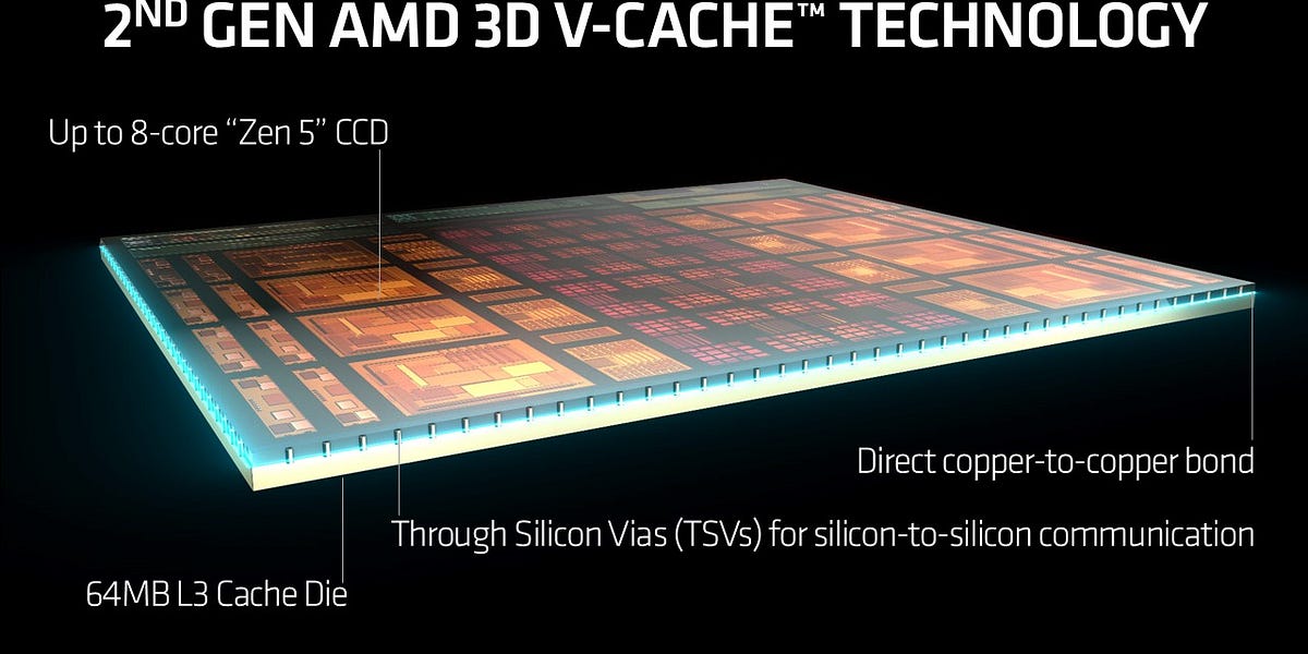
Following the first generation of V-Cache found in the Zen 3 and Zen 4 X3D SKUs, AMD is now following up with the second generation of V-Cache which is a major change for AMD in terms of packaging.
For the first generation of V-Cache, AMD took a standard Zen 3/4 CCD, thinned it to about 20 microns then stuck a die full of SRAM on top supported with 2 structural dies alongside the SRAM dies. With the second generation of V-Cache, AMD has moved the SRAM die down beneath the compute CCD.
With this move, AMD has gotten rid of the two support silicon dies. In order to fit the SRAM die under the compute die, not only does the SRAM die have 64MB of SRAM but also it now has additional power distribution under the CPU cores. The GMI link from the CCD to the IO die is unchanged but now it has to route from the CCD down to the SRAM die into the C4 bumps.
With the first generation of V-Cache, the voltage tolerances of the stacked cache was reduced. For example, the maximum voltage tolerance of the 7800X3D was 1.2 volts with a nominal voltage of 1.1 volts. But with the second generation of V-Cache, AMD has improved the voltage tolerance to the point that both the 9800X3D and the 9700X both have a maximum voltage of 1.4 volts and a nominal voltage of 1.28-1.31 volts.


