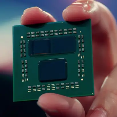
AMD 3D Stacks SRAM Bumplessly
Last week Computex Taipei 2021 was held virtually. While the event was largely a hit or miss among the chip vendors, one of the more interesting announcements that were delivered at the event was AMD’s 3D V-Cache – a 3D stacked SRAM. But while the stacked SRAM is interesting enough, the real announcement was the introduction of DBI into mass production in their highest-end chips by next year.
At the closing portion of the AMD event, AMD president and chief executive officer, Dr. Lisa Su went onto talking about some of the advanced technologies the company is working on. AMD disclosed their first application of true 3D chiplet stacking they called “3D V-Cache”.
A prototype chip was also shown at the event. AMD showed a Ryzen 5000-series microprocessor that incorporated the V-Cache. The Ryzen 5000-series microprocessors incorporate one or two Core Complex Dies (CCDs) along with an I/O Die (IOD). The V-Cache is a 64 MiB SRAM die that is said to be fabricated on TSMC’s 7-nanometer process. The V-Cache die is thinned and is then stacked directly on top of each CCD directly above the existing L3 cache area. On the Ryzen 5000-series microprocessors, each CCD features 32 MiB of L3 cache, therefore the V-Cache effectively triples the L3 capacity of each CPU. Two additional structural dies are added on top of the CCDs above the CPU complex. It’s unknown if those structural dies are blank silicon or if they include anything special (e.g., inactive thick copper traces which can enhance the thermal conductivity of the dummy die).
The 64 MiB 3D V-Cache die itself is measured 36 mm² (a 6 mm x 6 mm square). This is roughly 9 mm² more than the 32 MiB of L3 on the CCD which occupies around 27 mm² of silicon so the SRAM in the 3D V-Cache appears to be more tightly packed. Architecturally, the V-Cache die itself adds 64 MiB of SRAM capacity directly on top of the existing 32 MiB of L3 for a single, large, 96 MiB of L3 capacity. A complete chip with two CCDs would therefore have a maximum L3 capacity of 192 MiB per processor. The L3 bandwidth is said to be tripled to 2 TB/second while maintaining the same latency.


