Xilinx HBM2 Internals
HBM2 is a type of stacked memory, with each stack containing multiple DRAM dies (chips), and each die supporting 2 channels. Every channel accesses a different (and independent) set of DRAM banks - as a result, requests for one channel cannot access data from another channel. This can be thought of as each channel “owning” a certain address range. Channels may be clocked independently. For more details on HBM, see the Wikipedia article.
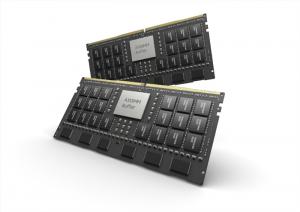
Xilinx’s HBM devices contain two Samsung Aquabolt HBM2 stacks with a 1024-bit wide bus (per stack). For the technical reader, I believe the 8GiB devices in particular have Samsung KHA844801X-MC12 HBM2 (16 banks; 2 channels per die.) Each stack has multiple dies, and each die has two channels - each of which is divided into two pseudo-channels with 64 bits of I/O each. Pseudo-channels operate in a semi-independent manner - reads and writes can be issued at the same time as other commands such as activations (“opening” a row for access) and precharges (“closing” a row after access.) Channels are independent, and may even be clocked independently.
Now, the HBM interface has 32 AXI3 1 ports (provides memory-mapped read/write access to a given portion of the HBM2 address space2). Each of these controls a single pseudo channel - this also means that sixteen of them go to one stack, and sixteen to the other. For an 8GiB (2x32Gb stack) device, every pseudo channel controls access to 2Gb (2^28 bytes, or 256MiB). For 16GiB (2x64Gb stack) devices, every pseudo-channel controls access to 4Gb (2^29 bytes, or 512MiB). It’s important to realize that every pseudo-channel is limited to its own section of memory - accesses through it cannot go to another pseudo-channel’s memory.2